Samsung Note 9 Schematic Diagram
Samsung j2 prime schematic diagram pdf Samsung manual schematics Samsung j2 prime schematic diagram pdf
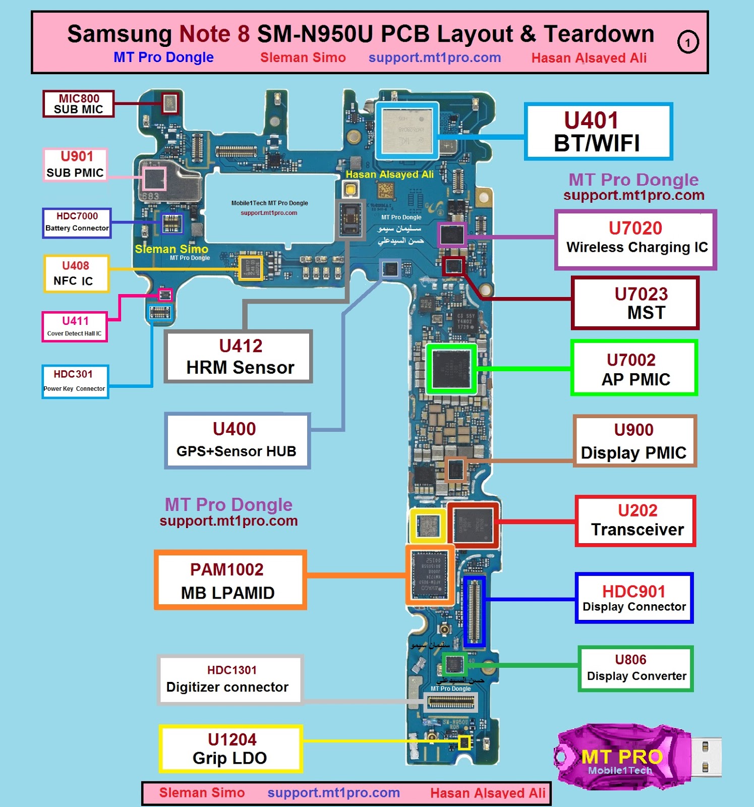
Samsung Note 8 SM-N950U Pcb Layout &Teardown
Samsung galaxy note10 sm-n970f schematics Samsung note sm layout pcb n950u Download samsung galaxy note 10+ schematics diagram
Schematics note10 n970f
Samsung galaxy note9 / sm-n960f schematicsSchematic samsung galaxy note 5 sm-n920 charger data hardware solusion Schematics n960f sm note9[view 39+] samsung note 4 schematic diagram.
[view 25+] samsung galaxy note 4 schematic diagramGambar schematic redmi note 9 terupdate Samsung m20 schematic diagram 339926-samsung m20 circuit diagramN920 garis jalur solusion sudah kasih menujukkan sebaiknya cek pada.

Schematics n920 samsung phonelumi
Schematic samsung galaxy note 4 hendsfree sm-n910 hrdware solusionSamsung galaxy note 5 sm-n920 schematics Samsung galaxy note9 / sm-n960f schematicsSchematics n920 phonelumi sơ đồ.
Download samsung galaxy note10 schematic diagramSamsung galaxy note 6 release date, price, specs, and features Samsung galaxy note 3 neo sm-n7505 schematicsGalaxy schematic circuit.

N910 solusion hrdware
Samsung galaxy note10+ schematicsN960f schematics note9 Samsung galaxy note10+ (sm-n975f) schematicsSamsung galaxy note10+ sm-n975f schematic and pcb layout (*.pdf).
N960f schematics note9Samsung note pcb sm n950u layout teardown Samsung galaxy note10+ sm-n975f schematic and pcb layout (*.pdf)Samsung note 8 sm-n950u pcb layout &teardown.

Samsung galaxy note 9 detailed teardown gives a glimpse of its internal components
Samsung galaxy note 9 sm-n960f circuit diagram service manual schematic схема :: service manualsJumper n950u j7 f1s u2ugsm oppo mic Samsung galaxy note internal note9 teardown components detailed glimpse gives its gizmochina n960u boardSchematic samsung galaxy note 5 sm-n920 charger data hardware solusion.
Samsung galaxy note9 / sm-n960f schematicsSchematics note10 n975u Samsung note 20 ultra schematic diagramSamsung note 8 sm-n950u pcb layout &teardown.
Samsung galaxy note20 ultra sm-n986u schematics
Samsung galaxy note 3 neo sm-n7505 schematicsSamsung galaxy note 5 sm-n920 schematics Thetechhacker releaseSamsung note 8 sm-n950u pcb layout &teardown.
Schematics diagrams m20Schematic n920 cek skema solusion charger jalur Samsung galaxy note8 sm-n950f schematicsSamsung galaxy note 9 schematic diagram and service manual.

Schematics samsung note 9 sm-n960n
.
.

SCHEMATIC SAMSUNG GALAXY NOTE 4 HENDSFREE SM-N910 HRDWARE SOLUSION - Dunia Blogger Indonesia

Samsung Galaxy Note 3 Neo SM-N7505 Schematics
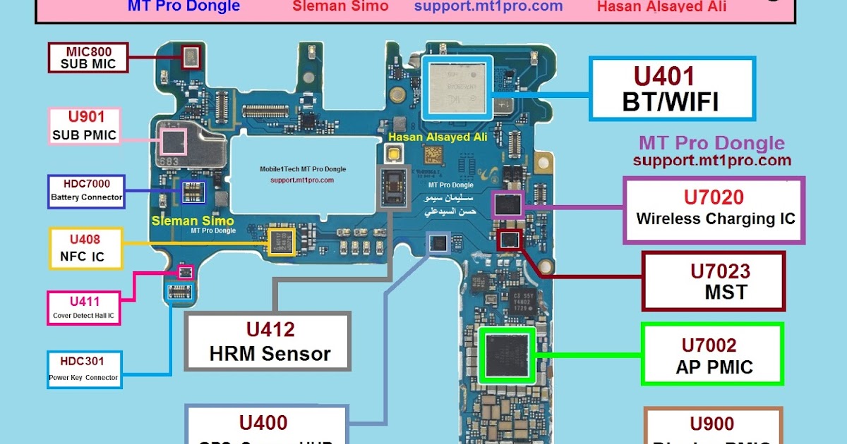
Samsung Note 8 SM-N950U Pcb Layout &Teardown

Samsung J2 Prime Schematic Diagram Pdf - IOT Wiring Diagram

Download Samsung Galaxy Note 10+ Schematics Diagram | Service Manual

Samsung Galaxy Note9 / SM-N960F schematics